| First put wafers in HMDS. Use HMDS recipe 5
for most situations, but use recipe #4 or 3 for wafers that will
immediately undergo long wet etches, like a 10 min BOE.
Let wafers cool for 5 minutes before applying photoresist,
and between each step below.
Use the dummy wafer to set your coater parameters. When
coating your wafer, choose a coater chuck slightly smaller
than your sample, in either Au or CMOS (red or green), contamination.
Never, EVER, use a chuck bigger in any direction than your
sample, as wafer vacuum will draw in photoresist, and ruin
the coater.
Always replace the dummy wafer on the CMOS chuck when done;
DO NOT leave with Au chuck!
DO NOT line the coater bowl with fabwipes unless ABSOLUTELY
NECESSARY.
Resist Choice.
Use pump #1 for OCG 825, a 1u positive photoresist (unexposed
areas remain after developing), pump #2 for AZ 5214 E,
a 1.5u image reversal photoresist (exposed areas remain
after developing), or pump #3 for AZ 4620 a 10u thick positive
photoresist.
Turn the resist dispense toggle switch off prior to setting
up the parameters, then turn on prior to coating actual
wafers. Dispense resist into bowl for two seconds prior
to use on wafer to clear nozzle tip of dried resist.
Coater recipes for OCG 825 and AZ 5214E:
Set dispense speed to ~500 rpm. Speed is adjusted while
the wafer is spinning, Using the dial immediately above
each of the three timers
Set spread speed to ~750 rpm
Set dispense and spread times to about 4 sec for pieces,
6 sec's for 4" wafers, or 8 sec for 6" wafers
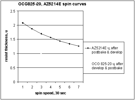
Set spin time to 30 seconds, and choose a speed to meet
desired resist thickness, (see chart attached) between
1500 and 5000 rpm.
Center dispense arm over wafer, then press start. When
done, wafer goes into teflon cassette for pre-bake.
Coater recipe for AZ 4620:
Set dispense speed to 0 RPM, and time to 12 sec for 4" wafers,
20 sec for 6" wafers
Set spread speed to 0 RPM and 10 sec
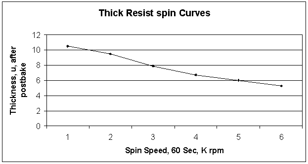
Set spin time to 60 seconds, and choose a speed to meet
desired resist thickness, (see chart attached) between
1500 and 5000 rpm.
Center dispense arm over wafer, press start. Do not allow
resist to reach the outside perimeter of wafer during static
(0 RPM) dispense, spread: if it does, it may get sucked
into the coater motor by wafer vacuum. Immediately after
the run, use a swab and remove the resist from the wafer
perimeter, before it dries and creates particulate contamination.
Last, put wafers into teflon cassette for pre-bake; consider
putting cassette in horizontally to limit resist contact
with cassette slots. You must double glove if touching
processing cassettes!
Clean Coater when Done:
When done with coater, you must immediately clean it.
Put the dummy wafer back on the CMOS chuck, set it to spin
at about 750 RPM continuously, and squirt acetone on the
bowl, and on the spinning wafer. After a while the bowl
should be clean of visible resist. Leave the dummy wafer
and CMOS chuck in place, turn power off.
Prebake:
Prebake at 90 C: 30 min for OCG 825 and AZ 5214 and 60
min for AZ 4620
Exposure:
EV1: Use about 2 seconds exposure for OCG 825 and
AZ 5214, and from 15 to 30 seconds for AZ4620, depending
on thickness. For exposures longer than 10 seconds, use
several intervals with wait steps to reduce resist heating.
Exposure times are 30% lower if mask is quartz
KS2: expose OCG825 and AZ 5214 for about 35 seconds,
AZ4620 for 500-700 sec, less for quartz masks.
AZ5214 additional steps: After initial mask exposure,
for image reversal resist, put wafers into post-exposure
bake (PEB) of 30min at 90C, then flood expose without a
mask for 45 sec (EV1) or 3 min (KS2)
Develop:
All developing should be done in a beaker just bigger
than the wafer, with NO MORE THAN about ¼" (1/2
cm) of developer. Thicker resists should be agitated in
a non-repetitive pattern, as the developing is diffusion
rate limited otherwise. Thin resists should only be lightly
agitated. In no case should developer ever slosh or splash
in the beaker! Wear protective gloves. Develop times are
always approximate, always develop to completion.
Develop OCG 825 in OCG 934 1:1 developer for about a minute.
Develop AZ 5214E in AZ 422 for about 2 minutes
Develop AZ 4620 in AZ 440 for about 4 minutes
If your develop time differs significantly, consider the
possibility of adjusting your exposure times (exposure
and develop times are inversely related)
Rinse wafers for at least one minute for thin resist or
two minutes for thick resist.
Microscope inspect:
Always check your develop results under a microscope before
post bake. Use low power, look for odd colors in the developed
areas. Check fine features under higher power last.
Post Bake:
Postbake OCG 825 for 30 min at 120C
No further PEB is needed for AZ 5214E
Postbake AZ 4620 for 30 min at 90C
 |